
 while minimizing energy consumption.")
As the demand for complex machine learning tasks continues to escalate, the neural network community has reached a critical juncture where traditional computing hardware is no longer sufficient to meet the burgeoning needs.
Photonic hardware has the potential to perform machine-learning calculations with reduced latency, offering a faster and more energy-efficient alternative. Although photonic gadgets can perform certain types of neural community computations efficiently, they are not capable of handling all forms of computation, necessitating the use of off-chip electronics or alternative approaches that compromise speed and efficacy.
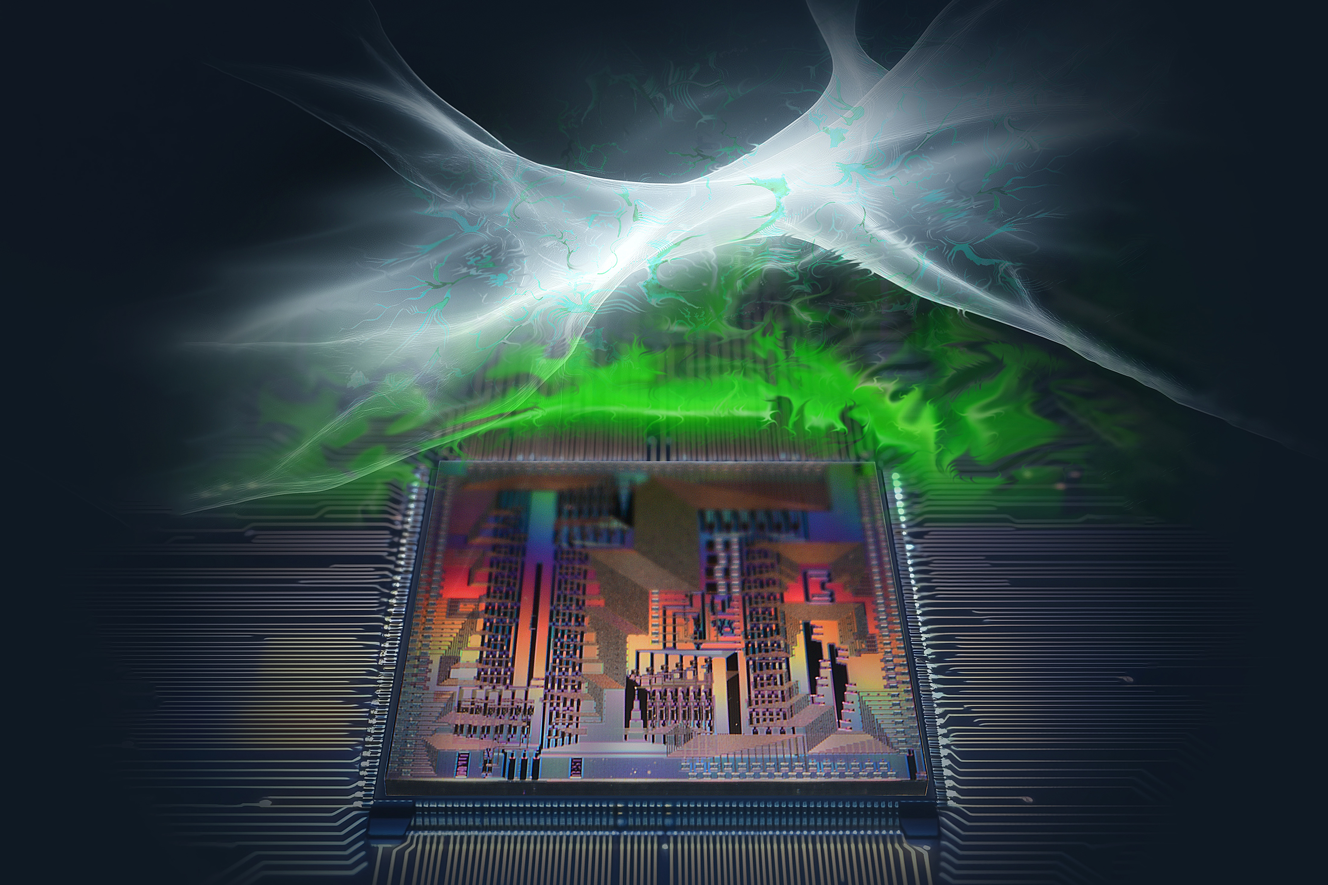
Scientists at MIT and other institutions have leveraged a decade’s worth of research to create a groundbreaking photonic chip that surmounts long-standing hurdles. Researchers have successfully showcased an integrated photonic processor capable of performing all crucial calculations required for deep neural networks on-chip in an entirely optical manner.
The optical gadget was able to complete the key computations required for a machine-learning classification process in less than half a nanosecond, achieving an accuracy rate of over 92 percent – performance equivalent to traditional hardware.
A novel chip, comprising interconnected modules that form an optical neural network, has been fabricated using industrial foundry processes, thereby enabling the potential for scalability and seamless integration with electronic devices.
The photonic processor has the potential to accelerate and significantly reduce energy consumption for complex tasks such as processing massive data sets in lidar applications, astronomical research, and high-speed telecommunications.
While model performance is crucial, it’s equally important to consider response speed. Now that we’ve successfully developed an end-to-end system capable of running neural networks in optics at a nanosecond time scale, we will begin contemplating functions and algorithms with greater depth,” says Saumil Bandyopadhyay ’17, MEng ’18, PhD ’23, a visiting scientist within the Quantum Photonics and AI Group at MIT’s Research Laboratory of Electronics (RLE) and a postdoctoral researcher at NTT Research, Inc., who is the lead author of a paper on the new chip.
Bandyopadhyay collaborates with Alexander Sludds ’18, ’19, ’23; Nicholas Harris PhD ’17; Darius Bunandar ’19; Stefan Krastanov, a former RLE analysis scientist turned assistant professor at the University of Massachusetts Amherst; Ryan Hamerly, visiting scientist at RLE and senior scientist at NTT Research; Matthew Streshinsky, former silicon photonics lead at Nokia now co-founder and CEO of Enosemi; Michael Hochberg, president of Periplous LLC; and Dirk Englund, professor in the Department of Electrical Engineering and Computer Science, principal investigator of the Quantum Photonics and Synthetic Intelligence Group and RLE, and senior author of the paper. The analysis
Deep neural networks comprise numerous interconnected layers of nodes, or neurons, processing and transmitting information to generate an output. Matrix multiplication is a fundamental operation in deep learning, leveraging linear algebra to propagate information through layers of interconnected neurons, transforming input data into meaningful representations as it flows downstream.
While performing linear operations, deep neural networks also execute non-linear transformations to enable the model’s ability to learn more complex and nuanced patterns. Deep neural networks are empowered by nonlinear operations, such as activation functions, to tackle complex problems effectively.
In 2017, a collaboration between Englund’s team and the research group led by Marin Soljačić, then Cecil and Ida Green Professor of Physics, enabled matrix multiplication using light.
Although the technology was available at that point in time, the gadget was still unable to perform nonlinear calculations directly on the integrated circuit. Precise optical data requires conversion into electrical signals, which are then transmitted to a digital processor to execute complex nonlinear calculations.
Nonlinearity in optics poses significant challenges due to the complex interactions between photons that fail to cooperate in a straightforward manner, rendering it a particularly intricate phenomenon. However, setting off optical nonlinearities proves arduously energy-consuming, making it challenging to develop a scalable system capable of achieving this feat.
By overcoming this hurdle, researchers developed novel units called nonlinear optical function units (NOFUs), seamlessly integrating electronic and photonic components to enable on-chip nonlinear processing.
Researchers developed an optical deep neural network on a photonic chip, comprising three layers of units that execute both linear and nonlinear processing tasks.
Initially, their system converts the parameters of a deep neural network into a concise format. An array of programmable beam splitters, as demonstrated in a 2017 paper, enables matrix multiplication by processing the input signals.
The data is subsequently transferred to programmable nano-fluorescence units (NOFUs), which exploit non-linear properties by harnessing a minute amount of sunlight and directing it towards photodiodes that convert optical signals into electrical currents. This course, eliminating the need for an external amplifier, consumes virtually no power.
We remain confined to the optical scope throughout, until we reach the top and must look away to obtain an answer. “This enables us to achieve ultra-low latency,” Bandyopadhyay explains.
By achieving submillisecond latency, they successfully established a real-time neural network on the chip, known as in-situ coaching – a process that can be notoriously power-hungry in traditional digital infrastructure.
“That’s especially useful for applications involving in-domain processing of optical signals, such as navigation or telecommunications, and also those that require real-time learning.”
The photonic system demonstrated outstanding performance, boasting over 96% accuracy in training simulations and an impressive 92% accuracy during inference testing, comparable to traditional hardware. While capable of performing key computations in less than half a nanosecond,
“This groundbreaking study proves that computational processes can be recompiled onto novel frameworks rooted in both linear and nonlinear physical principles, thereby enabling a vastly superior balance between computational power and required effort.”
The entire circuit was manufactured using the same infrastructure and fabrication processes employed to produce CMOS microprocessors for laptops. The novel technology could facilitate mass production of the chip by leveraging established methodologies that minimize errors throughout the manufacturing process.
Bandyopadhyay envisions that scaling up the device to integrate with real-world electronics, such as cameras or telecommunication systems, will be a crucial area of research in the years ahead. Researchers must identify and develop algorithms that capitalise on the advantages of optics to accelerate training methods and enhance their potency.
The study’s funding was partially provided by the United States government. Nationwide Science Basis, the U.S. Air Power Workforce of Scientific Analysis and NTT Analytics.