
Adjustments are coming to the Tensor G5 that was supposed to enhance the efficiency of the silicon. First, the Tensor G5 is being constructed by TSMC which is the biggest contract foundry on the planet. It is also being constructed on a barely extra superior course of node of 3nm promising the aforementioned enchancment in efficiency and energy-efficiency. To be extra particular, TSMC will probably be utilizing its third-gen 3nm node (N3P).
You’d assume that Google is taking the appropriate steps with the Tensor G5:
- Shifting manufacturing of the G5 from Samsung Foundry to TSMC.
- Utilizing TSMC’s third-generation 3nm course of node as a substitute of the 4nm node employed in the course of the manufacturing of the G3 and G4.
- Having Google design the appliance processor from scratch as a substitute of counting on a Samsung Exynos base.
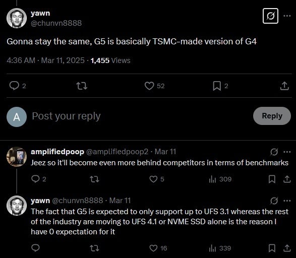
With the Tensor G5 anticipated to debut on the Pixel 10 line, you’d anticipate that such a landmark cellphone would function thrilling new options, and lately that would come with new AI capabilities. However earlier than you get enthusiastic about all of this, a tweet from @chunvn8888 states that regardless of the chances, the G5 will run on the similar efficiency degree because the G4. The one distinction will probably be that the G4 was manufactured by Samsung and the G5 will probably be constructed by TSMC.
The Tensor G5 utility processor may find yourself being a large let down. | Picture credit-X