
Amid a push by the Trump administration to have Intel Foundry Providers (IFS) carry extra contract semiconductor manufacturing to the U.S., early indications are that Intel’s 18A course of is holding its personal in opposition to TSMC’s first-gen 2nm node often called N2. Each course of nodes will go into mass manufacturing throughout the second half of this yr with IFS manufacturing a pocket book processor codenamed Panther Lake.
Tweets from Dr. Ian Cutress, who’s Chief Analyst at Extra Than Moore (a pleasant play on the final title of the person who co-founded Intel and got here up with Moore’s Regulation), an organization that consults with high semiconductor companies, present that Intel’s 18A SRAM density of 38.1MB/mm2 is identical determine being reported by TSMC. SRAM density is a measurement displaying the quantity of SRAM reminiscence that may be present in a given space of a semiconductor chip.
SRAM (Static-Random-Entry Reminiscence) is usually used in high-speed purposes reminiscent of CPU caches (L1, L2, L3). These high-speed layers retailer information that’s typically accessed in order that the processor does not have to attend for slower entry to the primary DRAM (Dynamic-Random-Entry Reminiscence) reminiscence. Increased SRAM density permits for bigger caches which, in fact, tends to enhance efficiency.
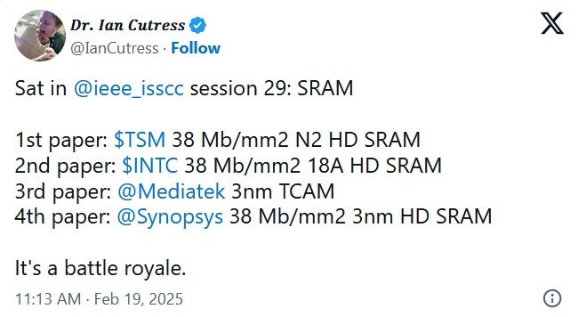
Intel and TSMC battle over course of management. | Picture credit-X
TSMC’s 2nm course of kicks off its use of Gate-all-around transistors (GAA) changing FinFET. Utilizing horizontal nanosheets stacked vertically, these transistors permit the gate to come back into contact with the channel on all 4 sides decreasing present leaks and leading to quicker speeds and better drive present. TSMC’s first-gen 2nm node delivered a 12% improve in SRAM density whereas high-performance SRAM density rose 18%.
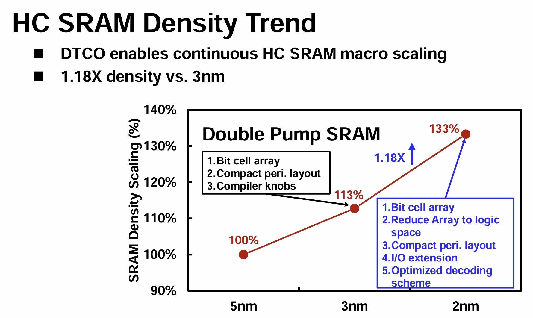
TSMC’s HD SRAM density is up 18%. | Picture credit-“X
Intel’s Energy Through function helps it enhance SRAM density for its 18A course of. Also referred to as BSPDN (Bottom Energy Supply), this system strikes energy supply networks (PDN) from the highest of the silicon wafer to the underside. The previous method took up an excessive amount of area limiting the SRAM density.
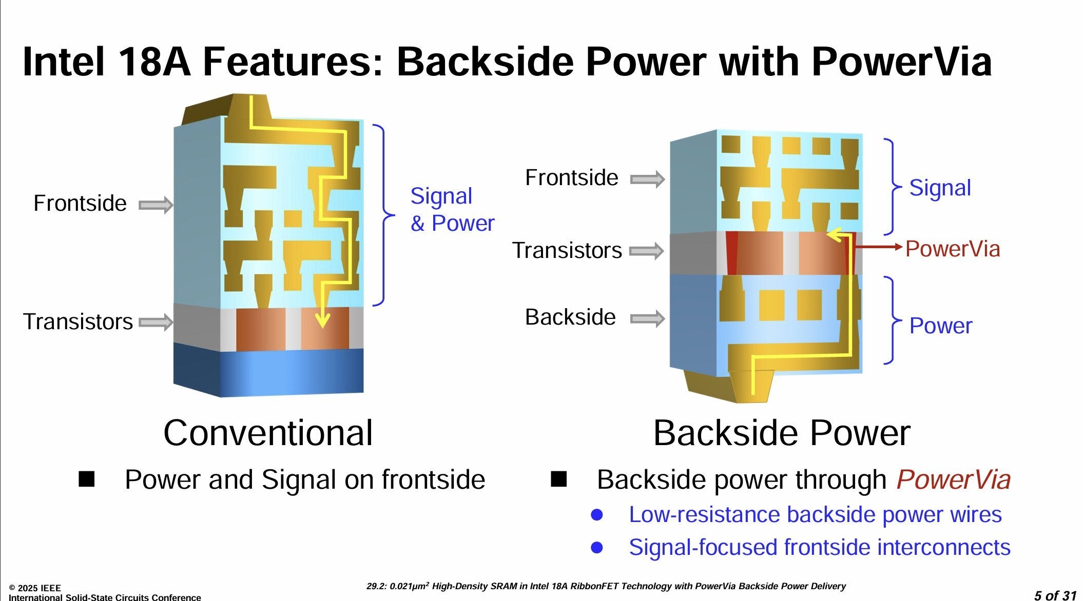
Intel’s bottom energy supply often called Energy Through helped its SRAM density at 18A. | Picture credit-X
It is vital to notice that the density figures can change relying on the construction of particular person SRAM reminiscence cells. The actual fireworks will come as soon as we see the outcomes of the 18A and N2 course of nodes within the type of precise parts used to energy new units.
Intel has signed up Amazon’s AWS which is desirous about utilizing the 18A node to supply chips for inside use with its information facilities and AI expertise. Microsoft and Broadcom are each additionally desirous about creating designs primarily based on 18A. Corporations displaying curiosity in TSMC’s N2 embrace the identical previous gang reminiscent of Apple, MediaTek, Nvidia, Qualcomm, and paradoxically, Intel.